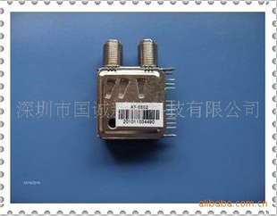
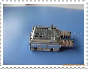
XT0502,高频头
- 型 号: XT0502
- 品 牌:国诚新特
- 价 格:≥1000:0.10元/个
- 产 能:大量供应
- 起订:1
- 交货期:7天
- 发布:深圳市国诚新特科技有限公司


- 联系人:杨其
- 主营:电视机
- 电话:8686026681-828
- 手机:13713961584
- 地址:中国广东深圳市龙岗区深圳市龙岗区坂田坂雪岗大道中兴路睿达科技园B栋六楼西

- 删除/纠错信息
产品详情
| 国诚新特 | 型号 | XT0502 | |
| 产品类型 | 标清 | 接收频道 | 950MHZ~~2150MHZ |
| 记忆数 | 1(个) | 功耗 | 0.7(W) |
| 电源 | DC-3.3V | 产地 | 广东省深圳市 |
| 材 | 金属外壳封装 | 电源电压 | DC-3.3V(V) |
| 制式 | DVB_S | ||
高频头XT0502为国诚新特科技自主研发的产品,其做工材料均采用元器件,电路板做工精细,工整,性能良。为保XT0502高产出,先后投入五十多万资金于检测设备的开发,力保每个产品在出厂前,都经过三道检测,为做到真正的全检模式,每个产品均贴有条码,每个产品的各项性能参数均可查看。其在使用功能上可完全取代夏普原装BS2S7HZ0502A.
DEVICE SPECIFICATION FOR XT0502
This specification covers L-band to I and Q base-band tuner intended for use in digital modulated satellite receiver(DVB-S).[1] General specification1-1 Receiving frequency range 950MHz to 2150MHz1-2 Input singal level per channel -75dBm to -25dBm1-3Nominal RF input impedance 75 ohm (F-connector)1-4Local frequency range 950 MHz to 2150MHz
1-5Channel Selection system PLL synthesizer(Clock:16MHz/4)1-6 Local step frequency 500kHz
1-7 AGC input voltage 0V to 3.3V
0V :
3.3 : Min gain
1-8 I/Q Output LPF cut off frequency(-3dB) 8MHz to 36MHz, variable(2 MHz step)
1-9 Nominal I/Q output level 0.5Vp-p at 1kohm load impedance
1-10 Nominal I/Q output impedance 50ohm
1-11 Operating Voltage B2,B4 3.3V± 0.15V DC
1-12Absolute maximum rating voltage B1A 25V DC, 400mA Max.
B2,B4 -0.3~4.0V DC
AGC,SDA,SCL -0.3~B2+0.3 V DC
1-13Circuit block diagram
1-14Connection diagram
1-15 Mass 25g
1-16 Storage condition Temperature 15 to 35
Humidity 25 %RH to 75 %RH
Period 6 months
1-17 Environmental characteristics RoHS compliant
(RoHS refers to the "DIRECTIVE 2002/95/EC OF THE EUROPEAN PARLIAMENT AND OF THE COUNCIL of 27 January 2003 on the restriction of the use of certain hazardous substances in electrical and electronic equipment.")
1-18 Attention items:
1) This unit contains components that can be damaged by electro-static discharge.
Before handling this unit, ground your hands, tools, working desks and equipment to
protect the unit from Electronic Static Destroy.
2) Avoid following actions;
a) to store this unit in the place of the high temperature and humidity.
b) to exe this unit to corrosive gases.
[2] Test condition
2-1 Supply voltage B2,B4 3.3V ± 0.1V DC
2-2 Ambient temperature 25℃ ± 5℃
2-3 Ambient humidity 65%± 5%
2-4 I/Q output level 0.5Vp-p(at 1kohm load)
[3] Electrical specification (Testing Condition is showed from 2-1 to 2-4)No | ITEM | SPECIFICATION | CONDITION | ||||
MIN | TYP | MAX | UNIT | ||||
3-1
| Noise Figure |
| 9 | 20 | dB | at AGC voltage=0V | |
3-2 | RF input VSWR |
| 2.0 | 2.5 |
| 950MHz to 2150MHz | |
3-3
| Gain deviation |
| 7 | 10 | dB | 950MHz to 2150MHz | |
3-4 | AGC control range | 72 | 78 |
| dB | AGC voltage: 0 to 3.3V | |
3-5 | 3rdorder intermodulation(2 tone) | 40 | 60 |
| dB | input level is -25dBm desired signal : Fo undesired signal : (Fo+29.5MHz,Fo+59MHz)or (Fo-29.5MHz,Fo-59MHz) LPF_Fc=20MHz | |
3-6
| I/Q phase balance | -4 | 0 | +4 | deg. | freq. offset is 100kHz | |
3-7 | I/Q gain balance | -2 | 0 | +2 | dB | freq. offset is 100kHz | |
3-8 | Pass band flatness of BB LPF |
|
| 2 | dB | 0.1MHz to fc×0.7 | |
3-9 | Local oscillator signal leak at RF input terminal |
| -68 | -63 | dBm | 950 to 2150 MHz | |
3-10 | Phase noise | 1kHz offset |
| -70 | -50 | dBc/Hz | measured at I/Q out |
10kHz offse |
| -78 | -76 | dBc/Hz | |||
100kHz offset |
| -85 | -78 | dBc/Hz | |||
3-11 | Reference leak |
| -40 | -30 | dBc | measured at I/Q out | |
3-12 | PLL lock up time |
| 10 | 50 | ms | within VT±5% VT is tuning voltage | |
3-13 | 1st Oscillator frequency error | -500 |
| 500 | kHz | -10℃ to +60℃ | |
3-14 | Current consumption | B2 3.3V |
| 200 | 215 | mA |
|
B4 3.3V |
| 25 | 40 | mA | |||
AGC |
| ±0.1 | ±1 | mA | |||
3-15 | Clock out level | 1.2 | 1.7 |
| Vpp | high impedance(*1) measured by FET probe | |
3-16 | Clock out frequency error | -80 | 0 | +80 | ppm | -10℃to +60℃ | |
3-17 | RF output VSWR |
| 2.0 | 2.5 |
| 950MHz to 2150MHz measured at RF out | |
3-18 | RF output gain | -5 | 0 | +5 | dB | ||
封装脚位图如下:
该会员还发布了以下产品:(查看更多)
-
XT7306
型号:XT7306
价格:≥1000:0.10元/个
-

XT7306(取代夏普高频头BS2S7VZ7306),高频头,国诚新特,Tune
型号:XT7306(DVB_S2)
价格:≥1000:11.00元/个
-

XT7306(取代夏普高频头BS2S7VZ7306
型号:XT7306
价格:≥1000:0.10元/个
-
XT0502,高频头
型号:XT0502
价格:≥1000:0.10元/个
-

XT0502(取代夏普BS2S7VZ0502),Tuner,高频头
型号:XT0502
价格:≥1000:0.10元/个
-

XT0502(取代夏普BS2S7VZ0502),接收机
型号:XT0502
价格:≥1000:0.10元/个
-

XT7306,高频头,国诚新特,Tuner
型号:XT7306(DVB_S2)
价格:≥1000:0.10元/个